

By Jonathan Trinastic, @jptrinastic
Spying on the Atomic Structure of Perovskites
Perovskites are darling materials in the world of solar cells but still somewhat of a mystery to scientists. Perovskite-based photovoltaics boast a combination of high performance and cheap production that makes them an ideal candidate to lead the next solar energy revolution. Like many young and talented upstarts, however, they don’t always perform consistently, and they burn out quickly. Scientists do not yet completely understand why, but they have taken an important step by creating the first images of individual atoms comprising perovskite crystals. These beautifully abstract images will hopefully illuminate how atomic changes cause perovskite solar cells to fail, and shed light on potential solutions.
A History of Promise and Frustration
The term perovskite refers to any compound with the chemical formula ABX3(A = CH3NH3), a lead ion (B = Pb), and bromide (X=Br), the perovskite quickly boasted light-to-energy conversion efficiency near 20 percent, immediately challenging the best contenders made of organic materials that had been refined for years.
There is just one problem: Perovskite-based solar cells degrade quickly—over the course of days—due to the organic molecules’ extreme sensitivity to water. Performance is also quite inconsistent, likely due to defects in the atomic structure that reduce the material’s ability to transport electrons and do useful work. Perovskites are also used as a thin film, only nanometers thick, which means that their surface structure plays an important role in determining photovoltaic (directly converting solar energy to electric current) performance. Although scientists have long known that defects and surface geometries were likely culprits of poor performance, so far no one had been able to peer into these atomic details of the perovskite crystal.
Surface Exposed
Now, for the first time, researchers have visualized the individual atoms making up the perovskite surface to begin exposing its secrets. To achieve this landmark result, scientists used a scanning tunneling microscope (STM). Like your finger probing a rough surface by running along its bumps and grooves, this microscope places a conducting tip extremely close to the material’s surface and then moves it across many different positions. As the tip passes a region dense with electrons, these negatively charged particles can jump (or “tunnel”) from the material to the microscope tip, creating a strong signal. By recording this signal across large surface areas, researchers get a glimpse of the periodic structure of the crystal and can infer the locations of each atom.
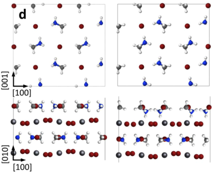
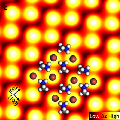
This STM image of glowing yellow spheres reveals the periodic, crystalline nature of the perovskite surface. A model of the atomic structure is superimposed over this image to show how the major atoms are arranged. The bright regions correspond to Br atoms (brown spheres) that are positioned much closer to the STM tip and thus produce a larger signal. The repetitive appearance of these bright signals corresponds to the repeated atomic arrangement of Br atoms that defines the crystal. The organic molecules (CH3NH3, white and blue atoms) sit between these Br atoms, in the darker regions, and are oriented perpendicularly to one another.
This perpendicular orientation of the organic molecules at the surface is surprising because it strongly contrasts the parallel configuration in bulk perovskite crystals. This indicates that the surface of the thin film significantly affects the geometry of the crystal. This seemingly small distortion can tune the electronic properties of the material and affect its light-harvesting ability. Surface atoms often rearrange in this way because each atom now has about half as many surrounding neighbors, creating a very different environment in which to find a position of equilibrium.
In addition to this surface rearrangement, other STM images reveal regions in the perovskite crystal where atoms appear out of place from the repeating crystalline pattern. These changes in position, known as “defects,” often appear as Br atoms shift from their regular position in the crystal lattice. Such defects can expedite deterioration of the cell and have a strong impact on the transport of electrons excited by light.
These surface changes and defects could be major players in the performance inconsistency of perovskite solar cells. However, this study analyzed only the atomic structure, and future studies will be necessary to understand these defects’ impact on solar cell efficiency. It is also important to note that this study was performed at low temperature (about -268°C), and significant atomic rearrangement can occur at room temperature. Therefore, future work should examine how these findings change with increasing temperature.
Scanning tunneling microscopy images, stark bursts of light reminiscent of spotlights at a sports stadium are more than an interesting form of abstract art. They reveal a reality to which our eyes are blind and about which we could only dream. With STM technology, we can now access the unusual world of atoms and better understand how perovskite surfaces impact solar cell performance. Both atomic reorientation and defects will change fundamental properties relevant to photovoltaics. Hopefully this visualization will be the first step in finding ways to tune the structure in our favor and push perovskite technology forward.
References
Ohmann, R. et al. Real-space imaging of the atomic structure of organic-inorganic perovskite. JACS, 137, 16049-16054, 2015.
Yang, S.Y. et al. High-performance photovoltaic perovskite layers fabricated through intramolecular exchange. Science, 348, 1234-1237, 2015.
Featured image courtesy of Contributing Photographer Steven Spence